You are here
Where is the Semiconductor Manufacturing Sweet Spot?
Where is the semiconductor manufacturing sweet spot? Two recent Semico Research Corp. studies provide the information to not only determine the overall sweet spot but to dig even further to find which products and technologies are the driving forces behind the growth or decline.
Chart 1, below, was developed from data in the fab database study. It shows the number of fabs operating and planned by wafer size.
Chart 1. Number of Fabs, Operating and Planned, by Wafer Size

Surprisingly, there are still more than 350 fabs operating at 150mm or smaller. Many manufacture trailing edge devices, especially discretes, while others manufacture relatively new devices, including analog, power, MEMS and LED devices. These semiconductors are not leading-edge devices, but they are essential to many electronics industry end-use products. The die size for many is quite small, and they do not scale well to smaller geometries. Many may continue to be manufactured in 150mm fabs for the immediate future. Others will undoubtedly migrate to 200mm fabs.
There were more than 150 fabs manufacturing devices on 200mm wafers in 2016. Many are producing MOS Logic semiconductors, but there is a sprinkling of 200mm fabs producing a wide variety of other semiconductor product types including analog semiconductors, MEMS devices, power semiconductors, and SRAM. Nineteen new 200mm fabs are planned or under construction.
There were more than 100 fabs operating at 300mm in 2016. These fabs are focused on high-volume devices manufactured at leading-edge technology nodes, including MPUs, DRAM, and NAND Flash. Following the usual pattern, many semiconductor product types will migrate from 200mm to 300mm fabs. More than 40 additional 300mm fabs are planned or under construction.
Chart 2, below, developed from data in the wafer demand study, shows wafer demand by technology node.
Chart 2. Wafer Demand by Technology Node
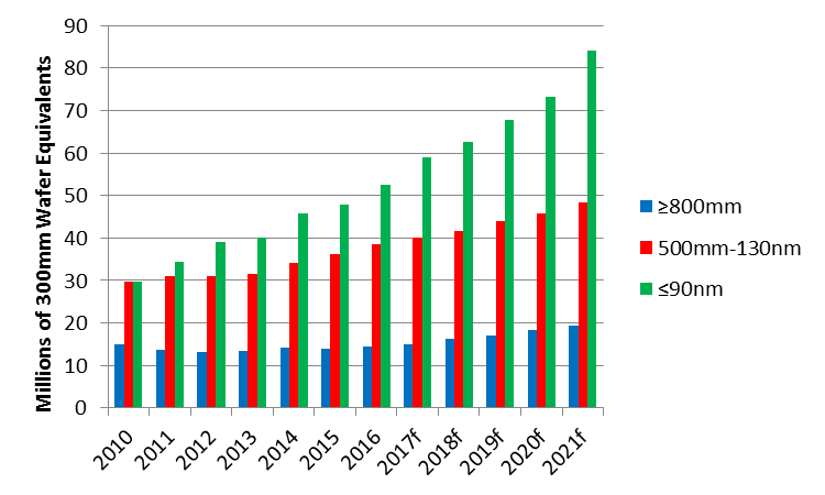
Source: Semico Research Corp.
The first category, greater than or equal to 800nm, was chosen because it represents most manufacturing in 150mm or smaller fabs. The second category, 500nm through 130nm, was chosen because it represents most manufacturing in 200mm fabs. The CAGR for 2016 through 2021 for this category is 4.6%. Most 300mm fabs are at technology nodes beyond 100nm, the third category. The CAGR for 2016 through 2021 for this category is 9.8%.
So, where is the semiconductor manufacturing sweet spot? It depends. The sweet spot for new fabs is 300mm, with 200mm fabs close behind. The sweet spot for wafer demand is 300mm wafers. Wherever your sweet spot is, Semico’s fab database and wafer demand studies have the data to help you find it. These studies are:
Contact Rick Vogelei at rickv@semico.com for more information.