You are here
Foundry Roadmaps: Real Solutions, or Just Hedging?
Major semiconductor foundries have revealed their advanced technology roadmaps for the next few years. They’re all investing billions of dollars into the development of process technologies and packaging options. The number of alternatives has been described as ‘dizzying’. How can all the foundries remain profitable? How does the customer decide which ‘route’ to take?

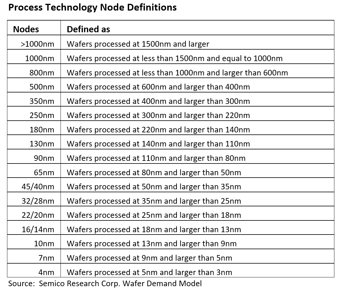
For the twenty-year period from the mid-1980s through the mid-2000s, process technology nodes were relatively easy to segment. Semico forecasted wafer demand into very clear process technology categories. Starting with the 45/40nm node in 2007, the two major logic manufacturers (Intel and TSMC) along with competing foundries began taking different paths. But the paths were still relatively clear. Intel rolled out their 45nm technology, and then TSMC rolled out their 40nm process. The foundries began to focus on low-power processes first. Then they followed up with their high-performance process several months to a quarter later.
Today, in addition to the number of different nodes, the challenge includes Intel’s claim that their 10nm process is comparable to the 7nm offered by other foundries. Semico believes the matching of product needs with process performance and cost will dictate market acceptance, not the marketing claims of technology-naming convention.

In May, Samsung revealed a full menu of processes that have been or will be released over the next few years. The new processes will be rolled out each year to provide new and existing customers with a variety of options to meet the competitive and broad product market application needs. In addition to their 10nm processes already in production, Samsung plans to offer risk production of 8LPP this year, 7LPP in 2018, 6LPP and 5LPP in 2019 and 4LPP in 2020. Samsung will also continue to offer a fully depleted SOI process. In fact, their roadmap includes an 18FDS, to be released in 2019.
Prior to Samsung’s Foundry Forum, TSMC provided a review of their process options at the TSMC Technology Symposium. In addition to 10nm being ramped this year, TSMC also has numerous new process technologies going back to 22nm and 12nm, as well as specialty processes for automotive, MEMS and CMOS image sensors.
At the April 2017 Technology Forum, TSMC announced they had 12 tapeouts lined up for 7nm in 2017. They also announced 8 design wins for the 16FFC automotive platform.
Most recently, GLOBALFOUNDRIES announced the availability of its 7nm (7LP) FinFET semiconductor technology. Design kits are available now, and the first customer products based on 7LP are expected to launch in the first half of 2018, with volume production ramping in the second half of 2018.
All three major foundries—TSMC, GF and Samsung—have publically addressed their rollout of EUV. In March 2017, TSMC provided their update on EUV showing successful, continuous throughput of 1400 wafers/day/machine at 125W source. They are confident that they will achieve acceptable throughput at 250W for their 7nm+ process. N7+ will include EUV layers and will be ready by 2018.
Samsung announced in early May they had demonstrated successful production at the targeted source power of 250W. In addition to a reduction of mask counts, Samsung expects to benefit from EUV with a much wider process window and smaller CD variation. Depth of focus and CD control improves the Samsung 7nm EUV process. In addition, the bi-directional patterning of M1 allows flexibility for metal pitch. Samsung expects to achieve 140 wafers per hour at 250W this year.
GF is investing in the addition of two EUV lithography tools in the second half of this year. The initial production ramp of 7LP will be based on an optical lithography approach, with migration to EUV lithography when the technology is ready for volume manufacturing.
Both TSMC and Samsung have stated that customers are requesting more options due to the broad market applications that are expected to roll out for IoT, automotive, industrial, deep learning, medical, and other emerging technologies. In addition to a larger number of process options, each foundry is offering a variety of packaging options.
It is interesting to note that GLOBALFOUNDRIES is making an impact with their 22nm FDSOI process. Semico believes this is true because both Samsung and TSMC have added more options to their roadmap to address the customers who require a low power non-FinFET option. Samsung has offered 28nm FDSOI in their portfolio for several years and recently added an extension of their SOI offering with an 18nm FDSOI process. TSMC has avoided the move to both PD and FD SOI and has opted to offer a 22nm process without FinFET. Their argument for non-SOI is that it provides an easier transition flow.
So is it too early to pick a foundry process winner or loser? Will all these technology offerings survive? Semico’s forecasts indicate an increased demand for foundry services across most technologies. There is definitely a need for the manufacturing capacity. So how does a fabless customer make a choice? Similar to our use of GPS to plan our route, we can select the shortest route or the fastest route and if traffic conditions change, we can take an alternative route, even if we’re halfway home. Just as there is not a single killer application, there is also not just one killer manufacturing solution. Each process and packaging option will be assessed based on the products targeted and the application. That also means there is not just one benchmark that will be optimal for every customer. Performance, power and cost are all key factors, but, in addition, there is a comfort factor that reaches into an instinctive analysis or hunch which is based on our past experiences and knowledge rather than conscious reasoning.
Based on that, Semico does not believe foundry market shares will make any significant shift in the next few years. Most likely a number of these processes and packaging options will not become mainstream or may not even survive. But we do believe that without a roadmap, you’re not even in the game.

