You are here
Ring of Fire Poses Risk to Semiconductor Manufacturing
There are hundreds of semiconductor fabs, spread all over the world. The trend over the past several years has been one of consolidation into several main manufacturing centers in the Asia/Pacific region, the United States, and Europe. Unfortunately for the industry, many of these fabs are located in areas prone to earthquakes. Some locations are also at an added risk of damage from tsunamis generated by earthquakes.
The northeast coast of Japan is a prime example; in March 2011, the region suffered a massive 9.0 magnitude earthquake and tsunami that killed 15,883 people, injured over 6,000, and left almost 2,700 still missing. The disaster also caused seven meltdowns at the Fukushima Daiichi nuclear power plant. The plant is still running on makeshift equipment and recently suffered a power outage that left four fuel storage pools without cooling water. In terms of damage to buildings, almost 130,000 buildings were completely leveled, and over a million others sustained some sort of damage. The amount of devastation was astounding, but the Japanese have done an amazing job of clearing away debris and recovering in the two years since, as illustrated by these photos posted at the Atlantic.
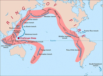
The "Ring of Fire" is an area of high seismic activity that extends from southeast of Australia north along the Pacific coast of Asia, crosses south of Alaska, and then continues south along the Pacific coast of North, Central and South America. According to Wikipedia, 90% of the world's earthquakes occur along the "Ring of Fire." Another 5-6% of the world's earthquakes occur along the Alpide Belt, which starts along the west coast of Indonesia, continues across the Himalayas, through the Mediterranean, and out into the Atlantic.
Figure: Ring of Fire Map (Source: USGS.gov)
 Semico Research considers fabs in Japan, Taiwan, and the west coast of the United States to be in the high-risk areas for earthquake activity. Thirty-nine percent of all fabs are in these high-risk areas, with another 22% in moderate-risk locations. In terms of capacity, 31% is in the high-risk areas, with another 36% in moderate-risk areas.
Recent quakes in Taiwan include a 6.5-magnitude temblor on March 4 that damaged some quartz furnace tubes and affected several thousand wafers. On March 27, a 6.1-magnitude earthquake shook buildings and caused damage to several DRAM manufacturers in Taiwan. TSMC briefly evacuated two fabs, one in Hsinchu and the other in Taichung. Operations were not affected at TSMC or UMC.
According to the head of Taiwan’s Seismology Center, this quake (along with two past quakes) may indicate the presence of a “blind” fault, or one as yet undetected. The fault could be more than 100km long, capable of producing a 7.0-magnitude or higher earthquake, and the potential for significant damage.
Taiwan is a key manufacturing center for the semiconductor industry, with two large foundries and most of their manufacturing capacity located on the island. So far, the benefits of location in terms of convenience and labor costs has outweighed the risks of being in the danger zone for earthquakes and tsunamis. Semiconductor fab building techniques help minimize risk of damage from earthquakes.
But it still makes sense to try to diversify manufacturing locations, and the supply chain as well, to minimize risk. For example, Intel has done an admirable job of spreading its fabs around the world, although its main R&D centers are on the west coast of the United States. Intel has fabs in Arizona and New Mexico, which are not prone to natural disasters of any kind. Its fabs in Ireland and Israel are also stable locations. The Dalian, China fab is located on a peninsula that would be more at risk of flooding from typhoons or tsunamis.


Add new comment