Semico IMPACT Conference: Focus on the IP Ecosystem
Doubletree Hotel, San Jose, CA November 6, 2013
To see videos of the speakers, click here.
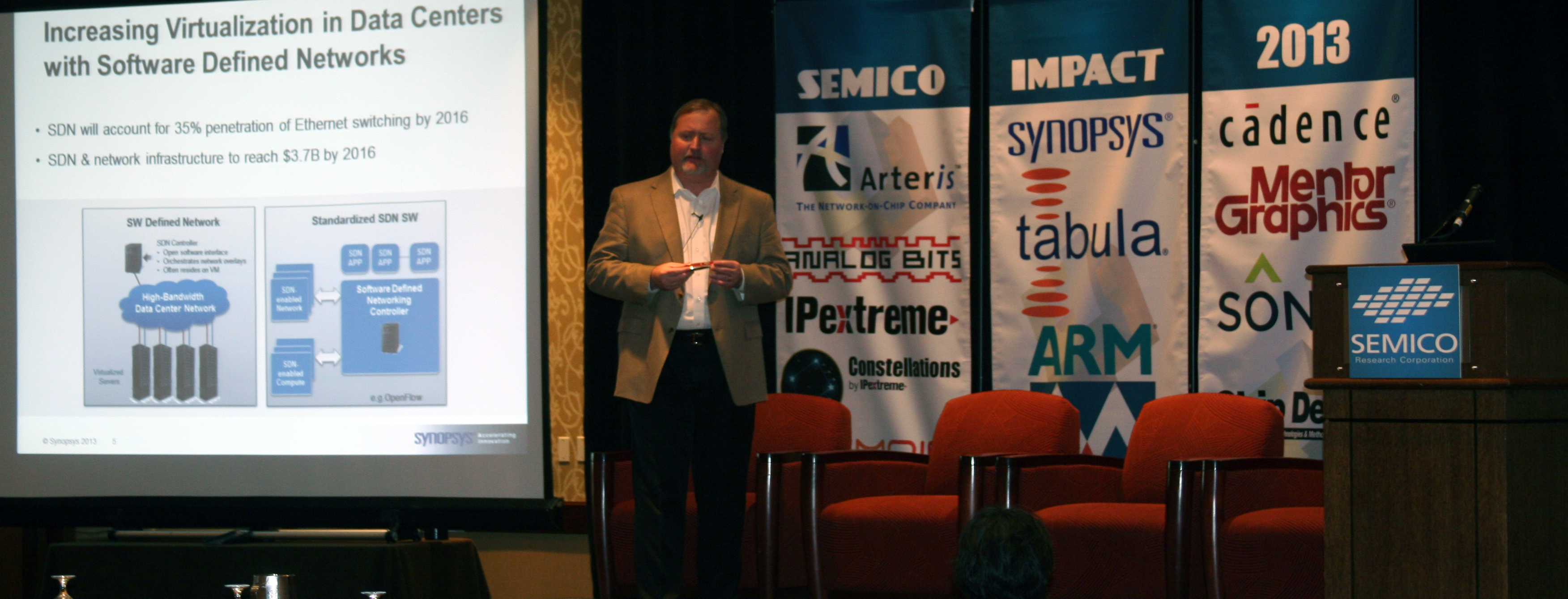
 Semiconductor IP continues to be a crucial component in the design and development of complex integrated circuits, especially SoCs. This Semico IMPACT Conference will focus on the IP ecosystem and issues that are affecting the growth of the semiconductor industry.
From Basic SoCs to Advanced Performance Multicore SoCs, designs are evolving into new forms, enabling a variety of enhancements to existing end applications.
- As device structures change and complexity increases, how are companies managing time-to-market versus chip complexity versus cost? Does it pay to wait?
- How do derivative designs drive new designs? Are new architectures postponed because of the availability of derivatives?
IP subsystems, the holy grail or marketing hype?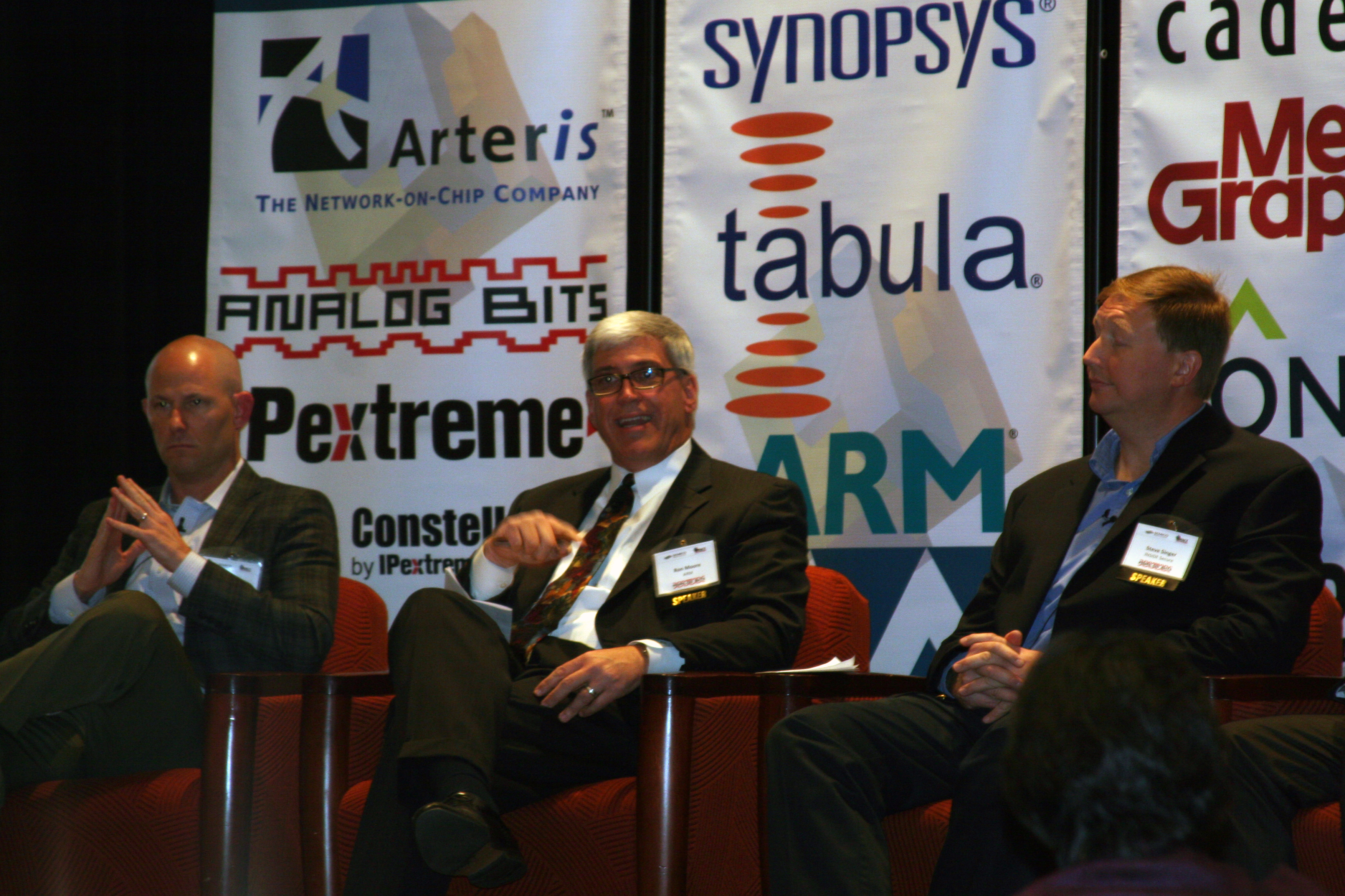
- What do third-party IP suppliers bring to the table that would encourage IDMs to pursue a "buy" versus "make" decision? Is a third-party IP subsystem a necessary evil or a productive way to solve design issues?
- Which IP subsystems are getting the most traction?
Changes in the IP market are prompting enhanced and more comprehensive tool sets from the EDA vendors. What can we expect in the future regarding more highly integrated and intelligent EDA tools to aid in infusing more complex IP blocks into SoC designs?
As designs become more complex, so too has the size of the verification effort. What is the current understanding of EDA vendors of this issue and what can be done about it? Where will it be in the near future? What do EDA and IP vendors see as the future of verification IP in relation to the total design effort? Will verification IP ever be used in the design of the SoC silicon itself? 
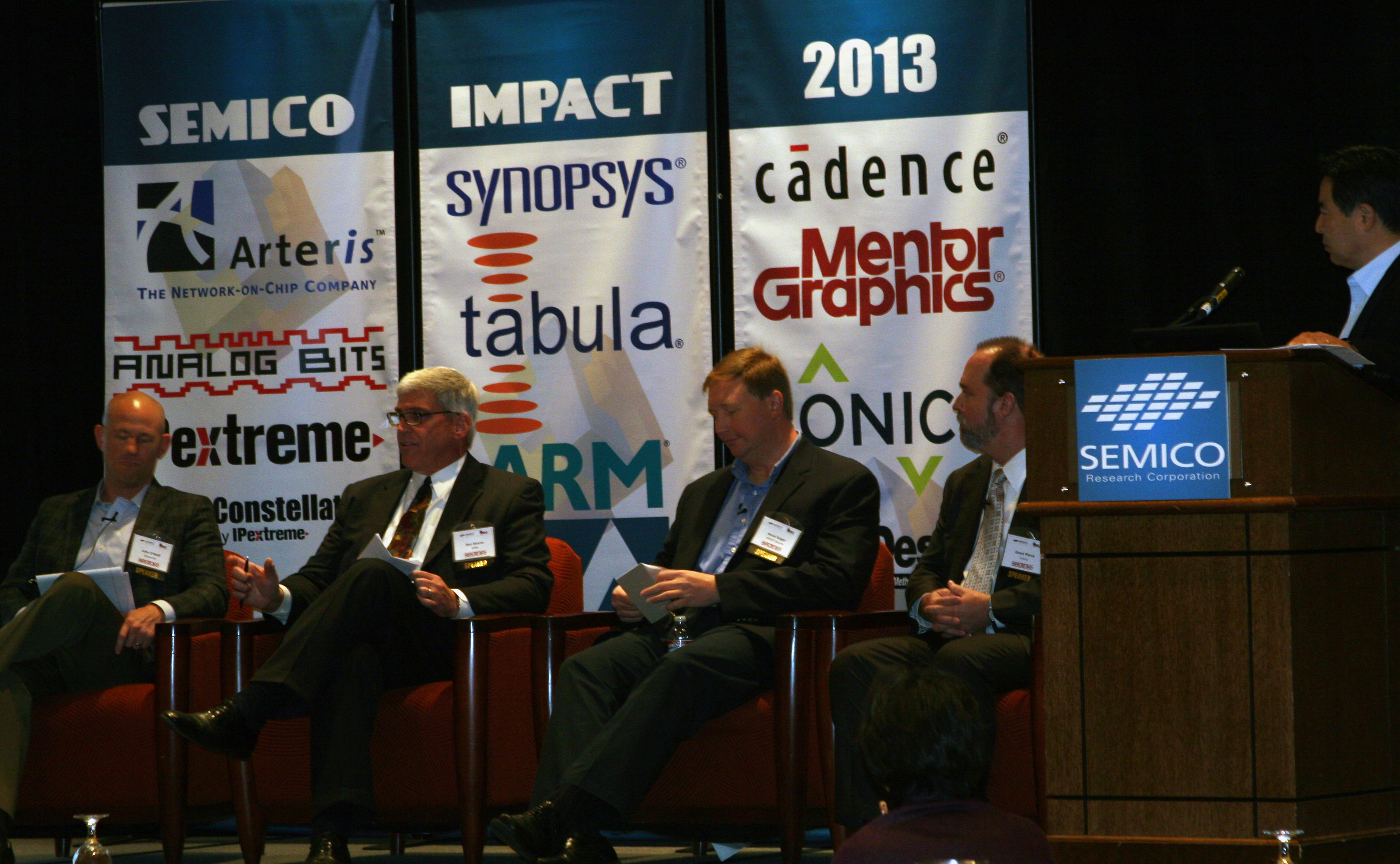
The Semico IMPACT Conference “Focus on the IP Ecosystem” will provide a lineup of thought-provoking keynotes and enlightening panels. If you are a silicon architect, an SoC designer or an ASIC design manager, plan to attend this event on Wednesday, November 6, 2013 at the Doubletree Hotel in San Jose, California.
EXPIRED - Join us for the next IMPACT Conference in 2014